
CENTER OF EXCELLENCE INTEL
| Name | Description | Instruments/Softwares |
|---|---|---|
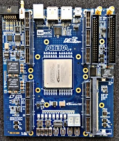
| DE5-NET FPGA Development Kit | The Terasic DE5-Net Stratix V GX FPGA Development Kit provides the ideal hardware solution for designs that demand high capacity and bandwidth memory interfacing, ultra-low latency communication, and power efficiency. With a full-height, 3/4-length form-factor package, the DE5-Net is designed for the most demanding high-end applications, empowered with the top-of-the-line Altera Stratix V GX, delivering the best system-level integration and flexibility in the industry. The Stratix® V GX FPGA features integrated transceivers that transfer at a maximum of 12.5 Gbps, allowing the DE5-Net to be fully compliant with version 3.0 of the PCI Express standard, as well as allowing an ultra low-latency, straight connections to four external 10G SFP+ modules. DE5-Net delivers with two independent banks of DDR3 SO-DIMM RAM, four independent banks of Cypress QDRII+ SRAM or functional compatible SRAMS provided by GSI and ISSI, high-speed parallel flash memory, and four SATA ports. The feature-set of the DE5-Net fully supports all high-intensity applications such as low-latency trading, cloud computing, high-performance computing, data acquisition, network processing, and signal processing. | 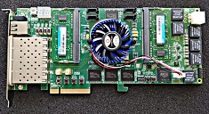 |
| DE4 FPGA Development Kit | The DE4 Development Board provides the ideal hardware platform for system designs that demand high-performance, serial connectivity, and advanced memory interfacing. The DE4 is powered by the Stratix® IV GX device. The evaluation of transceiver performance for jitter, protocol compliance, and equalization on the DE4, exceeded the Stratix IV GX performance standard with transceivers operating at 10 Gbps on SATA and HSMC interfaces. The DE4 is fully compliant with version 2.0 of the PCI Express standard in addition to serial ATA (SATA) interfaces making it possible to leverage the integration option for storage applications. DE4 also includes two DDR2 SO-DIMM socket supporting maximum capacity of 8-Gbyte of volatile memory for user applications which are capable running at 400 MHz clock rate. For large-scale ASIC prototype development, it can be established by a cable connecting to multiple DE4/FPGA boards through the HSMC connectors. | 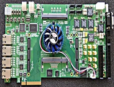 |
| DE3 Development Kit | The Altera DE3 ASIC prototyping development board allows researchers and engineers to access the high density and high performance FPGA - the Altera Stratix III. DE3 boards include the DE3-340 (338K logic elements) and the DE3-260 (254.4K logic elements) that are optimized with extra on-chip multipliers needed for DSP research and development. All of the DE3s can be stacked and all share the same set of function from the Terasic's daughter cards connected to them. Multiple DE3s can be joined together to increase design gate count and performance. |
 |
| DE2 Development Kit | The DE2 series has consistently been at the forefront of educational development boards by distinguishing itself with an abundance of interfaces to accommodate various application needs. Responding to increased versatile low-cost spectrum needs driven by the demand for mobile video, voice, data access, and the hunger for high-quality images, the new DE2-115 offers an optimal balance of low cost, low power and a rich supply of logic, memory and DSP capabilities. The Cyclone EP4CE115 device equipped on the DE2-115 features 114,480 logic elements (LEs), the largest offered in the Cyclone IV E series, up to 3.9-Mbits of RAM, and 266 multipliers. A High-Speed Mezzanine Card (HSMC) connector is provided to support additional functionality and connectivity via HSMC daughter cards and cables. For large-scale ASIC prototype development, a connection can be made with two or more FPGA-based boards by means of a HSMC cable through the HSMC connector. |
 |
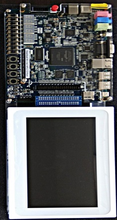
| DE1-SoC-MTL2 Development Board | The DE1-SoC Development Kit presents a robust hardware design platform built around the Altera System-on-Chip (SoC) FPGA, which combines the latest dual-core Cortex-A9 embedded cores with industry-leading programmable logic for ultimate design flexibility. Altera’s SoC integrates an ARM-based hard processor system (HPS) consisting of processor, peripherals and memory interfaces tied seamlessly with the FPGA fabric using a high-bandwidth interconnect backbone. |
 |
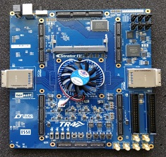
| TR4 Development Board | The TR4 Development Board provides the ideal hardware platform for system designs that demand high-performance, serial connectivity, and advanced memory interfacing. Developed specifically to address the rapidly evolving requirements in many high end markets for greater bandwidth, improved jitter performance, and lower power consumption, the TR4 is powered by the Stratix® IV GX device and supported by industry-standard peripherals, connectors and interfaces that offer a rich set of features that is suitable for a wide range of compute-intensive applications. The TR4 is supported by multiple reference designs and six High-Speed Mezzanine Card (HSMC) connectors that allow scaling and customization with mezzanine daughter cards. For large-scale ASIC prototype development, multiple TR4s can be stacked together to create an easily-customizable multi-FPGA system. |
 |
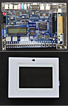
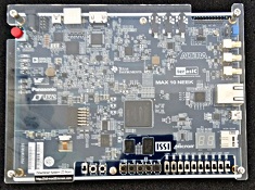
| MAX 10 NEEK | The MAX 10 NEEK from Terasic is a full featured embedded evaluation kit based upon the MAX10 family of Altera FPGAs. The MAX 10 NEEK delivers an integrated platform that includes hardware, design tools, intellectual property and reference designs for developing a wide range of audio, video and many other exciting applications. The fully integrated kit allows developers to rapidly customize their processor and IP to suit their specific needs, rather than constraining their software around the fixed feature set of the processor. The MAX 10 NEEK combines a 5-point LCD touch panel and digital image module that provides developers an ideal platform for multimedia applications, making the best use of the parallel nature of FPGAs. |
 |
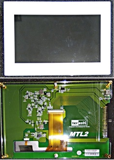
| Multi-Touch LCD Module(MTL2) | The Terasic Multi-Touch LCD Module Second Edition (MTL2) is an all-purpose capacitive touch-screen for your FPGA applications. It provides 5-point Multi-Touch support and a 7" color display LCD with 800x480 resolution. An IDE cable with an IDE-to-GPIO adapter (ITG) is provided in the kit to interface MTL2 with various Terasic FPGA development boards through a 2x20 GPIO interface. The kit provides everything that is needed to develop multimedia applications using a digital Multi-Touch panel. |
 |
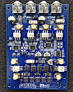
| Data Conversion Card | The AD/DA Data Conversion Card was created to provide a set of Analog to Digital and Digital to Analog interfaces including an Audio CODEC interface. The High Speed Mezzanine Card (HSMC) can be used to develop DSP applications with Altera Development boards and Terasic Development boards (e.g.DE3) that feature the HSMC connector. |
 |